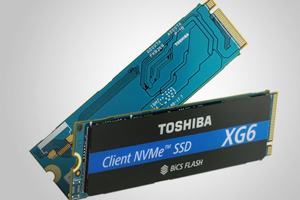
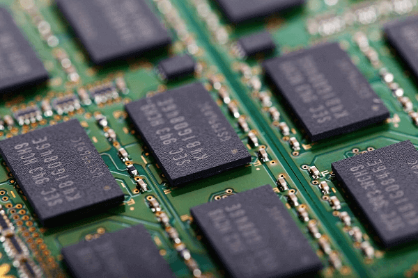
Want to get an SSD with larger capacity and higher performance to meet your needs? Now, Toshiba and Western Digital are preparing 128-layer 3D NAND memory that can bring large storage capacity and high performance to SSD. Read this post to learn more information on the 128-layer 3D NAND chip.
3D NAND Layer
3D NAND flash is a type of flash memory where the memory cells are stacked vertically in multiple layers, which can achieve higher density, lower power consumption, better endurance, lower cost per gigabyte and faster speed.
Since the advent of 3D NAND technology, particle manufacturers have been working on the stacked layers, starting with 32-layer, then 64-layer, 96-layer. At present, the most advanced technology is 96-layer 3D NAND.
Now, more advanced technology will be coming. You may have heard the news: Toshiba and Western Digital 128-layer 3D NAND memory.
Toshiba and WD 128-layer TCL 3D NAND Flash Chip
It is reported that Toshiba and its strategic ally – Western Digital are jointly developing high-density 128-layer 3D NAND TLC flash memory. In the nomenclature of Toshiba, the memory chip will be called BiCS-5.
Larger Capacity
The interesting thing is that in spite of the spatial density, the chip will implement TLC (3 bits per cell) rather than the newer QLC (4 bits per cell). Probably this is because NAND flash manufacturers are still worried about the low yields of QLC memory chips. In total, the 128-layer 3D TLC BiCS-5 NAND can offer the capacity of 512Gb per chip, which is equivalent to 64GB.
To put it simply, adding more layers to this type of flash can add more capacity per die, which is similar to building a house, for example, increasing the number of floors on a building would cause more available rooms/floor space.
Previously, the BiCS NAND of Western Digital was able to offer a total of 96 layers but now move to 128 layers, delivering 33% more capacity than the 96-layer chip. And makers can use the technology to create higher capacity NAND flash chips, or develop smaller chips that have the same capacities as before, reducing the cost of each chip in the production process.
Reportedly, the Toshiba and Western Digital 128-layer 3D NAND memory will hit commercial production in 2020-2021.
Higher Write Performance
According to Toshiba and Western Digital, the new BiCS-5 3D NAND flash chip features a 4-plane design. It has a layout of four separate sections or planes, each of which can be independently accessed, as opposed to BiCS-4 memory that uses a two-plane structure.
Besides, this new chip reportedly doubles the write speed per unit-channel: from 57MB/s to 132MB/s.
Smaller Size
In addition, the chip uses Circuit-under-Array (CuA) that is a design innovation in which the logic control circuits are in the lower plane, with data layers stacked above. Because of this, the dimensions of the crystal are reduced by 15% compared to the flash memory without CuA.
Aaron Rakers, the Senior industry market analyst at Wells Fargo, says that Toshiba and Western Digital offer the industry a high chip density with 85% yield of the plates per 300mm wafer.
Toshiba and Western Digital 128-layer 3D NAND Memory Will Reduce Cost
By decreasing die area usage and offering higher stacks of 3D memory, Western Digital is enabling its memory division to offer more storage capacity per unit of die area, reducing the cost/GB of the future memory chips.
This will make the memory chip cheaper to produce and also increase the production volume (in terms of GB produced). In turn, this will lead to higher capacity memory chip production and lower NAND pricing.

